So while we are in awe, there is some group of engineers that are going "hey grandkid, let me tell you about Mylar memory. They pushed the envelope back in the day. It would be nice if some of these articles would have names so we could go "wow Bob, that was some amazing engineering".
If you want names, transformer read-only storage was originally invented by T. L. Dimond in 1951 and used by Bell Labs. At IBM Hursley Laboratory, Antony Proudman was responsible for memory development including TROS.
As I've pointed out before, the early history of computing was a struggle to get enough memory. Any kind of memory. IBM had an electronic multiplier in test before WWII. Eckert, at Columbia University, built some incredible semi-programmable kludges out of IBM tabulator equipment. (He went on to be one of the designers of the UNIVAC I.) But memory remained insanely expensive, more than a million dollars a megabyte, into the 1970s, 30 years after the first all-electronic arithmetic unit.
Confusingly, there were two unrelated Eckerts in early computing. Wallace Eckert was an astronomer at Columbia who figured out crazy ways to use punch card accounting machines to do scientific computation, and wrote the book "Punched Card Methods in Scientific Computation".
Presper Eckert, who was unrelated to Wallace Eckert, is the better-known co-designer of the groundbreaking ENIAC computer (along with Mauchly). They then designed the UNIVAC I, basically the first successful commercial computer.
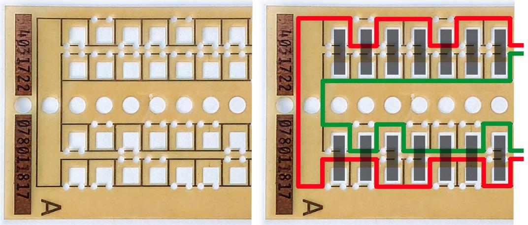
It's a sheet of Mylar that has had conductive traces deposited on it, forming wires. This means it can be bent to go around curves without the use of additional connectors.
The interesting thing to me about the TROS sheets is that they were initially manufactured to be the same [0] but were programmed by punching out (cutting) the traces in places to zig-zag the current path either through a transformer loop or around it. Presumably there was a machine that positioned a punch to the correct position, based on coordinates from an input punch-card deck, before descending and cutting through the traces.
[0] Note that there are two designs - one with the inputs on the left and one with the inputs on the right, to line up on the connector block to the diodes. Although it's possible it's the same design, just flipped before the punching step.
Strangely enough, there are three tape designs that have the conductors offset slightly. The stack of Mylar tapes cycles through the three designs. The purpose is to prevent wires in neighboring layers from being parallel, which would cause stray capacitance.